
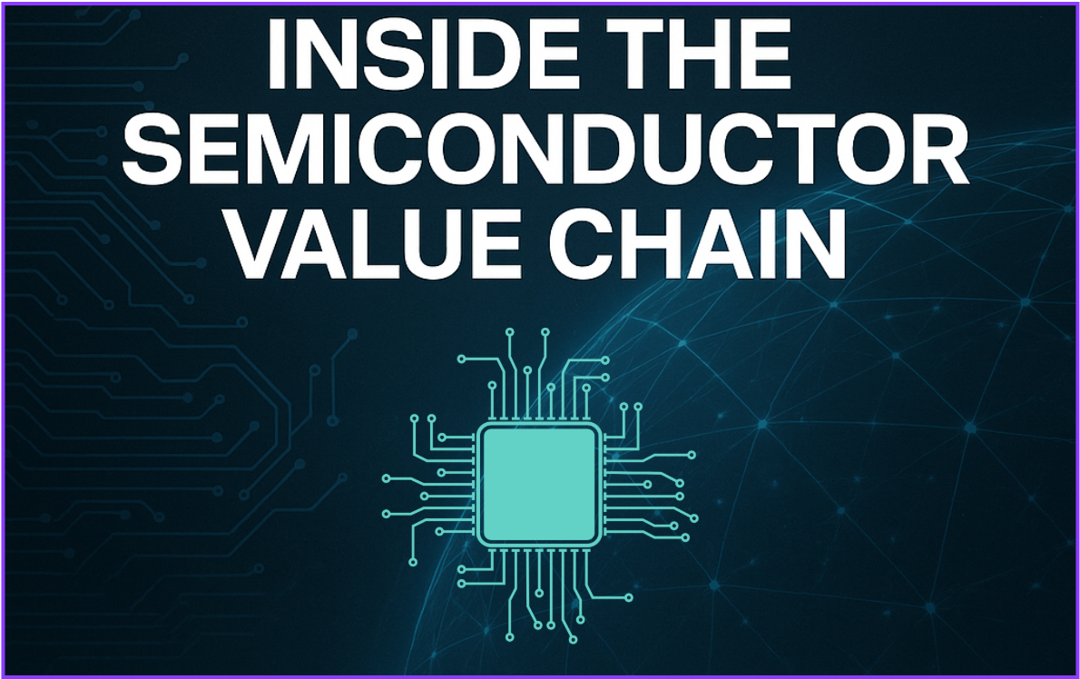
Key Steps Involved in Bringing Semiconductors to Life
This is the second edition of our semiconductor newsletter series. Last week, we traced the fascinating origins of semiconductors, from the invention of the first transistor to the rise of pioneers like Shockley, Fairchild, and the Traitorous Eight who laid the foundation of the invisible engine that runs our electronic devices today. This week, we move from history to hardware. We will be unpacking the full semiconductor value chain, step by step, from chip design to fabrication to final testing.
The Semiconductor Value Chain – FOUR Key Steps
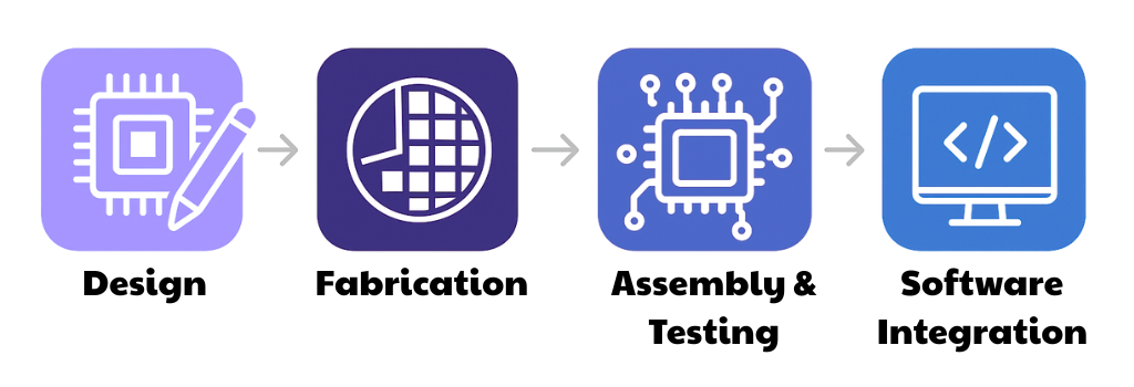
1. Semiconductor Design
Designing a semiconductor is very much similar to building a house. Imagine you want to build a house. Before you lay a single brick, you hire an architect to design it. They decide things like, How many rooms you need, Where the doors and windows go, How the plumbing and electricity will run, etc… etc…
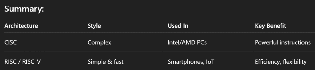
Chip Architecture: Before starting to design the chip, engineers need to answer a crucial question: Which kind of “language” or “Instruction” style will this chip understand? In technical terms, this is call the “Chip Architecture”. Think of it like rules for the computer brain, it tells a chip to read and execute instructions like, add these numbers or move this data or run this app, etc. Even more simply, chip architectures are different ways to talk to the processor. Without getting into complex details, following are TWO (Complex Instruction Set Computer – CISC and Reduced Instruction Set Computer – RISC or RISC-V) of the most commonly used chip architectures and some basic diffenentiating details:
While designing a chip engineers design tiny electronic brains that live inside your phone, car, or laptop. Just like an architect, they use powerful softwares to plan things like, What the chip should do (e.g., process photos, connect to Wi-Fi, play games, etc), How the billions of tiny components (called transistors) are arranged on it, How fast and energy-efficient it will be, etc… etc… Practically, this process isn’t as straightforward as it sounds. It takes months and sometimes even years to design chips.
Final Output: A detailed file, like a construction blueprint which will be sent to a factory to begin making the chip (Fabrication).
2. Fabrication
Once the architecture is finalised based on which the chip is designed, now comes the actual construction. The actual manufacturing of a chip happens in a ultra-clean, high-tech factory which in technical terms is called a “foundry”.
Like we use bricks and cement to construct a house, foundrys use “Silicon Wafers”. Simply explained, silicon wafers are thin, shiny discs made from super-pure sand. These are processed using extremely precise machines in the presence of certain chemicals and gases.

The blueprint (design) is projected onto the wafer using light, like stenciling. In this process, layers of metal and silcon compounds are added, patterned, and etched away. This process is repeated hundreds of times, adding millions or billions of transistors onto each chip. It’s like baking a 100-layer cake, where you carefully stack ultra-thin layers of materials and carve out circuit patterns. What’s fascinating is that each layer is 1,000 times thinner than a human hair.
Photolithography: It is a technical term for a tool that is used to draw patterns. In simple terms, “Photolithography” is using light to draw incredibly tiny shapes on the silicon wafer, shapes that eventually become transistors, wires, and logic gates inside the chip. Following are the steps involved in Photolithography.
Start with a clean wafer > Coating the wafer with photoresist > Shine extreme UV light through a mask > Light hardens parts of the photoresist > Wash away soft parts > Etch the pattern to form trenches or channels.
Final Output: A silicon wafer full of many tiny, unfinished chips (called DIES).

3. Assembly, Packaging & Testing – Making Chips Usable
After the silicon wafer comes out of the foundry, it now has a lot of miniature brains on a wafer. But you can’t plug a wafer into your phone, you need to slice, wrap, and test them before starting to use them. Following are the steps:
Cutting: The wafer is cut into individual dies (each one is a chip), just like cutting the cake from a tray into small pieces which can be sold individually.
Packaging: Each die is enclosed in a tiny plastic or ceramic case with metal legs or contact points. This protects the chip and allows it to be connected to a circuit board. To continue the cake analogy, each piece of the cake which was cut in the above step, is put into a wrapper.
Testing: Each chip is tested to check if it works and the broken ones are thrown away. Again the cake analogy, you check if any piece is burnt before shipping the same to customers.
Final Output: Finished, tested chips that can be sold and shipped.
4. System/Software Integration – Bringing Chips to Life
At this step, the chip is ready, but does nothing on its own. It’s like a brain in a jar, powerful, but useless until it’s put into a body and connected to nerves. Therefore, the chip is now placed inside a device (phone, car, laptop, etc.) and a software is written to control it. This is like telling the chip when to wake up, how to communicate with other parts, and what actions to perform.
For example, a chip in your phone that helps run your camera. The phone company writes a code that tells it how to adjust focus, optimize lighting, compress video, etc. In cars, chips manage everything from braking systems to music players.
Final Output: A complete, functioning device, powered by the chip.
Conclusion
As we close out Part II of our exploration into semiconductors, it becomes clear that the journey from design to system integration is nothing short of an intricate, symphony of precision, and collaboration. Each step in the value chain, Design, Fabrication, Assembly & Testing, and System Integration, plays a vital role in powering the devices that define modern life. While Part I traced the roots of this industry and honored the visionaries who laid its foundation, this edition simply breakes down the value chain of the semiconductor ecosystem.
Next week, we’ll turn our attention to the companies that operate in various parts of the value chain that we discussed today and their business models. We will also see how various functions in this complex industry is controlled only by a handful of players. Till then, Happy Investing!!!
Disclaimer: These insights are based on our observations and interpretations, which might not be complete or accurate. Bastion Research and its associates do not have any stake in companies mentioned. This newsletter is for educational purposes only and is not intended to provide any kind of investment advice. Please conduct your own research and consult your financial advisor before making any investment decisions based on the information shared in this newsletter.
🤣MEME OF THE WEEK🤣
